New thin-film solar panels cheapest and cleanest and getting better yet Dr. Mae-Wan Ho
Photovoltaic (PV) technologies are progressing rapidly in boosting efficiency and bringing manufacturing costs down; simultaneously, their environmental indicators are also improving.
A recent lifecycle assessment (LCA) of PV technologies based on data of rooftop installations under Southern European insolation (incident solar radiation) of 1 700 kWh/m2/y found an energy payback time (EPBT ) of 1.7, 2.2, 2.7 and 1.1 years respectively for ribbon-silicon, multicrystalline silicon. monocrystalline silicon, and thin-film CdTe (cadium tellurium) systems [1]. (EPBT is the time it takes for the device to generate as much energy as had gone into producing it, see [2] Which Renewables? SiS 39).The EPBT of the CdTe PV was much smaller than the other systems although its electrical-conversion efficiency was the lowest at 9 percent, compared with 11.5 percent for ribbon, 13.2 percent for multicrystalline, and 14 percent for monocrystalline silicon.
A follow-up study updated the LCA and presented the ‘cradle-to-gate’ emissions of GHG and heavy metals of the same four commercial PV systems based on the most recent data (2004-2006) [3]. These are largely indirect emissions associated with the use of fossil fuels in the lifecycle of the PVs. Direct emissions of heavy metals from mining and smelting are also included, whereas liquid and solid wastes are for the most part being recycled, and so were not considered in the study. The choice of electricity and fuel sources is important in determining the total emissions.
For silicon PV, the data from 11 commercial European and US PV module manufacturing companies were supplemented by numbers from the literature. Each module assembly typically consists of 72 0.125 m x 0.125m solar cells with silver contacts ini front and back sides. Ethylene-vinyl acetate and glass sheets encapsulate the PV module to protect it from the elements during operation. Crystalline silicon modules typically have aluminium frames for additional strength and easy mounting.
The lifecycle of silicon PV modules start with the mining of quartz sand. The silica in the quartz sand is reduced in an arc furnace to obtain metallurgical grade silicon, which is then purified further into electronic grade or solar grade silicon. This is done either by the Siemens process in which a reactor with silane and hydrogen gases are heated to 1 100-1 200C for growing silicon rods, or the modified Siemens process in which the silane and hydrogen gases are heated to ~800 C.
Data from CdTe PV modules in commercial production were from a manufacturing plant in Perrysburg Ohio in the United States. The typical frameless CdTe modules are 1.2 m x 0.5 m with electricity conversion efficiency of 9 percent (though this has increased to 10 percent by September 2007).
Cd is obtained from a waste stream of Zn smelting. Te is recovered from the slimes produced during electrolytic copper refining. Cd is further purified either through leaching and vacuum distillation, or through electrolytic purification followed by melting and atomization or vacuum distillation. Te is also further purified by the same methods. CdTe is produced finally via proprietary processes.
The CdTe absorber layer and cadmium sulphide (CdS) window layer are laid down by vapour transport deposition based on subliming the powders and condensing the vapours on glass substrates. A stream of inert carrier gas guides the sublimed dense vapour cloud to deposit the flims at 500-600 C with a growth rate of 1 micrometre per second. The interconnections and back contacts are formed by depositing a layer of common metals followed by series of scribing and heat treatment
The results of the lifecycle emissions using different databases are presented in Figure 1. Case 1 is the current electricity mixture in Si production, CrystalClear project and Ecoinvent database. Case 2 is the Union of the Co-ordination of Transmission of Electricity (UCTE) grid mixture and Ecoinvent database. Case 3 is the US grid mixture and Franklin database. The conditions used are the Southern European average insolation of 1 700 kWh/m2/y, a performance ratio of 0.8 and a lifetime of 30 years. The performance ratio is the real output of energy compared with the theoretical maximum output.
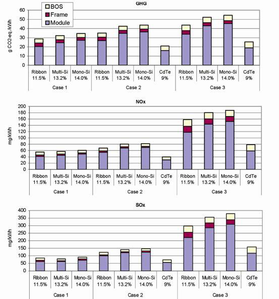
Figure 2. Lifecycle emissions from silicon and CdTe PV modules.
BOS is the Balance of System (module supports, cabling and power conditioning).
As can be seen, the CdTe PV module gives the lowest ghg emissions at just over 20 g CO2 equivalent per kWh. It also gives the lowest emissions of nitrogen oxides and sulphur oxides.
The CdTe PV can emit Cd both directly and indirectly, whereas the crystalline Si PV would emit these only indirectly. The total direct Cd emissions from the lifecycle of CdTe PV modules coming from mining, smelting, purification of the element and the synthesis of CdTe are 0.015 g/GWh. The total direct emissions of Cd during module manufacture are 0.004 g/GWh. Emissions during accidental releases such as fires are extremely small, if any. The total direct emissions of Cd make up 0.02 g/GWh.
Indirect Cd emissions come from the generation of electricity used in producing all parts of the PV module, for providing heat and mechanical energy during materials processing, for climate control of the manufacturing plant, and for transport of materials and products. The Cd is contained in fossil fuels burnt, a fraction of which is released into the atmosphere during combustion. The dominant sources of such indirect Cd emissions are from coal burnt during steel-making processes and during glass-making from the boiler materials and from the electricity supply needed in the boiler.
The results show that CdTe PV actually prevents a significant amount of Cd from being released to the atmosphere. Every GWh electricity generated by CdTe PV module can prevent about 4 g of Cd emissions. The direction emissions of Cd during the lifecycle of CdTe PV are 10 times lower than the indirect emissions, and about 30 times lower than those indirect emissions in the lifecycle of crystalline PVs.
There is major scope for improving the environmental indicators while simplifying the manufacturing processes and reducing costs. For example, thin-film modules can be manufactured by ink-jet printing techniques and flexible metal sheets used as substrate [2].
Article first published 01/08/08
Comments are now closed for this article