Graphene’s unusual electronic structure enables it to produce remarkable quantum coherent effects even at room temperatures, opening the door to new applications in electronics and spintronics Dr. Mae-Wan Ho
It all began when Konstantin Novoselov, Andre Geim, and colleagues experimented on thin films of one to several layers of graphene isolated with sticky tape or simply by rubbing graphite, i.e., drawing, on a hard surface [1].
The ability to control the electronic properties of a material by applying an external electric field (gate potential) is at the heart of modern electronics. This enables one to vary the concentration of charge carriers in a semiconductor device and hence the electric current passing through it. Like many other condensed matter physicists, Novoselov and Geim were on the lookout for new materials that would do better than silicon in the semiconductor industry, as silicon is nearing its limit of performance (see [2] The Computer Aspires to the Human Brain, SiS 58).
The researchers started by looking for electric field effect in graphene; and found the biggest, fastest, and most coherent one ever observed in any material. They demonstrated quantum Hall effect (see Box) occurring even at room temperature, something that hitherto, one could only see at very low temperatures in the highest quality, most carefully crafted electronic devices. As fellow graphene researchers commented, the observation of these stunning effects [3] “in a material fabricated by such a pedestrian technique, sparked a firestorm of interest that continues to this day.”
Quite apart from the range of potential applications of graphene (see [4] Graphene & the New Age of Carbon, SiS 59), it is the basic science that arouses the most passion.
The experiments of Novoselov, Geim and colleagues [1] showed that electrical conductance increases linearly and symmetrically as the gate potential applied is increased from 0V in either direction, positive and negative, indicating that the charge carriers switch between electrons and holes. This ‘ambipolar’ electric field effect is seen in other semiconductors, but never as large; and the current does not decrease to zero at the minimum (0V), where the charge carriers are a mixture of electrons and holes.
At the same time, quantum Hall effect (see Box) was found at three different temperatures: close to absolute zero, 70K and 300 K (room temperature) [5]; thereby extending the previous temperature range for quantum Hall effect by a factor of 10. The reason that quantum Hall effect can be observed even at room temperature is due to the highly unusual nature of the charge carriers in graphene, which behave as massless quasiparticles referred to as ‘Dirac fermions’ described by Dirac’s equation that combines quantum mechanics with special relativity; the Dirac fermions travel in high densities ~1013 cm-2 at 1/300 the speed of light through thousands of interatomic distances without scattering.
The Hall effect is the production of a voltage difference (the Hall voltage) across an electrical conductor, transverse to an electrical current in the conductor and in the presence of a magnetic field perpendicular to the current. It was discovered by Edwin Hall in 1879. The Hall coefficient is the ratio of the induced electric field to the product of the current density and the applied magnetic field, and is a characteristic of the material of the conductor, as its value depends on the type, number and properties of the charge carriers of the current.
The presence of a magnetic field perpendicular to the direction of motion of the moving charges exert a force on the charges, causing their paths to become curved, so that excess charge accumulate on one face of the material, leaving equal and opposite charges exposed on the other face, creating an electric field that opposes the migration of further charge.
A quantum Hall effect is the quantum mechanical version observed in two-dimensional electron systems in which the Hall conductivity s takes on quantized values:
 (1)
(1)
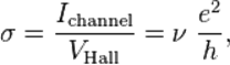
where Ichannel is the channel current, VHall is the Hall voltage, e is the elementary charge, h is Planck’s constant, and n is the filling factor that can take on either integer or fractional values. The quantum Hall effect is referred to as the integer or fractional quantum Hall effect depending on whether n is integer or fractional. The integer quantum Hall effect is simply explained in terms of single-particle orbitals of an electron in a magnetic field. The fractional quantum Hall effect is more complicated, as its existence relies fundamentally on electron-electron interactions, and is understood in terms of charge-flux composites known as composite fermions. The quantization of the Hall conductances is incredibly precise, being integer or fractional multiples of e2/h up to nearly one part per billion.
Figure 1 shows a room temperature quantum Hall effect obtained by Novoselov, Geim and team [5].
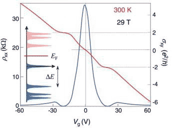
Figure 1 Quantum Hall effect at 300 K and 29 Tesla magnetic field
The Hall conductance sxy (right vertical axis and red curve) measured perpendicularly to the magnetic field as a function of gate voltage Vg applied reveals plateaus at 2e2/h for both electrons and holes in the positive and negative directions respectively; the left vertical axis (and blue curve) shows the magnetoresistance rxx in the direction of the current flow, which goes to zero at the plateaus of the Hall conductance. This is the signature of the quantized Hall effect. The inset shows the quantized energy Landau Levels (LL) of the charged particles in magnetic fields. The large energy gap DE between the Fermi level EF (the highest LL energy state of the electrons) and the lowest exceeds the thermal energy kT by a factor of 10. In addition, the very high carrier concentrations of up to 1013 cm-2, with only a single 2 dimensional sub-band occupied, and the high mobility of the charge carriers - which does not change from liquid helium to room temperature - remaining at ~10 000 cm2/Vs, all contribute to the survival of the quantum Hall effect at room temperature.
Finer details of the quantum Hall effect of graphene were observed by Philip Kim and his team at the University of Columbia New York in the US in experiments carried out at liquid helium temperature 1.6 K. They varied the magnetic field from 1 to 10 Tesla and held the gate potential constant at 15 V; or held the magnetic field constant at 9 Tesla and varied the gate potential from -80 V to +80 V. This enabled them to observe multiple plateaus in Hall conductance sxy beyond the two found by Geim and Novoselov’s team, including one that was not previously observed at 0V, a point (Dirac point) where charge carriers switch from holes to electrons [7] (Figure 2).
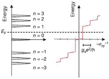
Figure 2 Landau Levels of graphene and fractional quantum Hall effects (modified from [7])
Interestingly, the plateaux of sxy occur at half-integer values of the Hall conductances, a highly unusual form of fractional quantum Hall effect. The plateaux appear between LL levels and jumps when a level is crossed. In graphene, sxy takes on the quantized values:
sxy = +gs(n + ½) e2/h (2)
where +gs(n + ½) = n, the filling factor (see Box) is in half-integer values, n is the index of the Landau Level, and gs is the degeneracy (number of quantum states with the same energy). The first plateau at n= 0 for electron and hole is situated exactly at +gse2/2h. As the Fermi level (adjusted by the gate voltage) crosses the next electron (or hole) LL, sxy increases (or decreases) by an amount gse2/h, giving the quantization condition in equation (2). In a later publication reporting investigations with stronger magnetic fields and better samples of graphene [8], the degeneracy was shown to have a value of 4: 2 arising from the 2 sublattices of carbon in graphene and 2 from different spins of the electrons. Splitting of the degeneracies gave rise to extra quantum Hall plateaux. Splitting of the spin degeneracy at the Dirac point is particularly interesting, as it leaves two co-existing edge states circulating in opposite directions with opposite spins (see Fig. 3 below).
The half-integer quantum Hall effect is accompanied by a non-zero Berry phase, a quantum phase acquired in the course of a cycle, which could provide the basis for new applications in electronics and spintronics [3, 7].
The half-integer quantum Hall effect and non-zero Berry phase were both theoretically predicted by other researchers, and stem from the unusual electronic structure of graphene; which also accounts for all its other extraordinary properties.
Graphene is a two-dimensional sheet of one carbon thick atoms arranged in a honeycomb crystal lattice, each atom bonded to three neighbours by strong s bonds formed by the hybridisation of the 2s, 2px and 2py atomic electron orbitals of carbon [3, 9]. The remaining out of plane 2pz or p orbital determines the low-energy electronic structure of graphene (see later).
The covalent s bonds are responsible for the planar structure of graphene and are the strongest chemical bonds known, accounting for the mechanical strength of graphene and also for the its high thermal conductivity (see [4]).
The 2D planar structure and the unusual massless charge carriers that can be excited in high densities by low energies (tens to a hundred volt) make graphene chemically very sensitive, and hence ideal for chemical detection and biosensing. It has been demonstrated that the Hall conductance of a micrometre sized graphene flake is sensitive to the absorption or desorption of a single gas molecule.
The optical properties of graphene stems directly from its planar structure and zero band gap. For photon energies larger than ambient temperature and the highest (Fermi) electronic energy, optical conductivity – the increase in electrical conductivity due to absorption of light - is a universal constant independent of frequency, G = e2/4ħ, where e is the electron charge and ħ is Planck constant divided by 2p. Consequently, all other optical properties - transmittance, reflectance, and absorptance (opacity) - are universal constants. And the ratio of absorbed to incident light for graphene is simply proportional to the fine structure constant (a = e2/ħc ~1/137): P = (1 - T) ≈ pa = 2.3 %, where c is the speed of light. This makes graphene the most transparent and strongest film available. For a few layers of graphene the opacity increases in multiples of 2.3 %.
Graphene’s electronic and macroscopic quantum properties can be explained by the energy band structure created by the p orbitals which spread out to form two energy bands: the bonding (lower energy valence band) and anti-bonding (the higher energy conduction band). A representation of the energy band structure around each carbon atom in the crystal lattice is shown in Figure 3a. The bonding-anti-bonding gap closes at six points called K points or Dirac points, the geometry around those points are cones (Fig. 3b), which explains why electrical conductance increases linearly as energy (gate potential) goes up in either positive or negative directions.
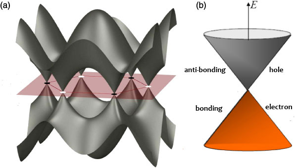
Figure 3 The energy band structure of graphene (see text)
The electronic structure rapidly evolves with the number of layers, approaching the 3D limit of graphite already at 10 layers. Only graphene and to a good approximation, its bilayer have the simple electronic energy spectra of zero-gap semiconductors with one type of electrons and one type of holes. For 3 and more layers, the spectra become increasingly complicated. Several charge carries appear and the conduction (anti-bonding) and valence (bonding) bands start notably overlapping.
It is clear that explorations on the amazing quantum feats of graphene as well as its chemically modified forms have only just begun.
Article first published 15/07/13
Comments are now closed for this article