Developing graphene for flexible easy to manufacture and affordable photovoltaic applications Dr. Mae-Wan Ho
A key process in getting electricity from light is the creation of excited electron-hole pairs of charge carriers on the absorption of light. The efficiency of the process depends substantially on what happens to the excited charge carriers; efficiency can be greatly enhanced if instead of losing the energy as heat (or phonons), the excited charge carriers use their excess energy to produce more electron-hole pairs through carrier-carrier interaction or scattering processes. An international team of researchers led by Jan Tielrooij and Frank Koppens at Institut de Ciéncies Fotoniques, Barcelona, Spain, have made measurements showing that carrier-carrier scattering does predominate in graphene exposed to light over a wide range of wavelengths, resulting in the production of secondary ‘hot’ electrons from the conduction band that can drive electric currents, thereby greatly enhancing the efficiency of photon-electricity conversion [1].
The unique properties of graphene that make it an efficient photon-electricity converter are its zero band gap, flat light absorption spectrum and strong electron-electron interactions (see [2] Why Graphene is Amazing, SiS 59). Theoretical work has already suggested that graphene can create multiple electron-hole pairs from a single absorbed photon during relaxation of the primary photo-excited electron-hole pair. Instead of losing the excess excitation energy as heat or phonons, it transfers the energy to other electrons to create hot charge carriers. But exactly how efficient this process is in practice is not known.
The team of researchers used an ultrafast light pulse in the optical range to ‘pump’ (excite) the graphene system, followed by a probe in the teraHertz (1012 Hz) region (below visible) to follow the dynamics of the excited electron-hole pair through changes in the transmission of the probe after different delay times [1].
The intrinsically doped graphene sample consists of a monolayer grown by chemical vapour deposition (see [3] Graphene from Greenhouse Gases to Save the Climate, SiS 59) and transferred onto a quartz substrate. From other measurements, the Fermi energy (energy of the least tightly held electrons) was determined to be 0.17 eV, which corresponds to an intrinsic carrier concentration of 2 x 2012 cm-2.
The ultrafast light pulse was applied at varying wavelengths to pump the sample. And the response to the probe after different delay times was recorded. The transmission of the probe first rises approximately linearly reaching a peak at a delay time ~2oo fs (femto second = 10-15 s), then decays over a longer timescale ~1 400 fs. This is explained as follows. During the initial rise carrier-carrier scattering between the photoexcited carriers and other carriers in the Fermi level promotes those carriers from below to above the Fermi level, creating hot carriers up to the peak at ~200 fs when the photoexcited carriers have relaxed, and a hot-carrier distribution is established. Subsequent relaxation of the hot carriers occurs on a much longer time scale.
They found that the density of carriers excited goes up linearly with absorbed photon density, as well as with the photon energy (when absorbed photon density is kept constant) over a range that span almost an order of magnitude in photon wavelength from the infrared (1.6 eV) to the ultraviolet (4.65 eV). The two ways of achieving a hotter distribution of carriers are interchangeable: either by increasing absorbed photon density or by increasing the photon energy. This is a clear signature of the dominance of carrier-carrier scattering. The results were reproduced with a model, which predicts that the number of secondary hot electrons scales approximately linearly with photon energy, and that 9 additional hot electrons are created for every photoexcited electron; and are promoted from below to above the Fermi level in the conduction band, and hence can contribute to electricity.
The results indicate that the transfer of energy from photoexcited carriers to other carriers is efficient over a wide range of frequencies from infrared to ultraviolet. This sets graphene apart from conventional semiconductor systems where the frequency range is limited by the bandgap. Furthermore, the number of secondary hot electrons is expected to be highly sensitive to the doping level, which can be manipulated to enhance quantum efficiencies and give tunable energy transfer over a wide spectral range.
The theory sounds promising, but in practice, it is not easy to realize the full potential of what graphene can achieve in harvesting sunlight for electricity.
The most ambitious attempt to tap into the potential of graphene is the creation of an all carbon solar cell fabricated from a combination of graphene with other carbon allotropes (molecular forms) that have in the news not so long before: fullerenes and carbon nanotubes.
All-carbon-based devices have already been demonstrated, such as an all-carbon nanotube-based hand-held field emission display [4], transistors composed of a semiconducting single-walled nanotubes or nanoribbons of graphene [5] and an all-carbon micro-supercapacitor made of graphene (see [6] Graphene Micro-Supercapacitors for On-Chip Energy Storage, SiS 59).
Fullerenes have been incorporated into organic photovoltaics (OPVs) since 1995, and high electron affinity fullerene derivatives are commonly used acceptor material in OPVs [7].
A solar cell with an all-carbon active stack of single-chirality semiconducting single walled nanotubes as light-absorber and electron donor and C60 fullerenes as acceptor was constructed, and had a maximum power conversion efficiency of just 0.1 % under the standard testing condition of AM (airmass) 1.5 100mW/cm2 illumination [7].
One major problem in processing CNTs and fullerenes is that they are only soluble in a limited number of toxic organic solvents. A team led by Jiaxing Huang at Northwestern University Evanston, Illinois in the US used the readily soluble graphene oxide made by chemical exofoliation from graphite as surfactant to help dissolve SWCNT and fullerenes in water, resulting in a colloidal suspension that could be spin-coated into smooth thin films 1 – 2 nm thick. (Spin coating is a process for depositing a uniform thin film on flat substrates. A small amount of the coating material is applied at the center of the substrate, which is rotated at high speed in order to spread the coating material by centrifugal force.)
To construct a solar cell, a layer of the C60/SWCNT/GO film 5-8 nm was spin cast onto an indium tin oxide (ITO) glass substrate coated with a smooth 20 nm film of poly(3.4-ethylenedioxythiophene):poly(styrenesulfonate ) (PEDOT:PSS) as hole transport layer. Heat annealing at 150 ºC activated the insolating composites by partially reducing GO into graphene. Next an additional film of C6o was thermally evaporated onto the top as a blocking layer to prevent carbon nanotubes from bridging opposite electrodes, and as an electron transport layer. Finally, 100 nm thick aluminium electrodes were deposited to complete the device. This device gave maximum power conversion efficiency (PCE) of 0.21 %. Replacing the C60 blocking layer with C70 resulted in a dramatic improvement of PCE to 0.85 % [8].
All carbon devices are attractive not just because of the unique and remarkable properties of the carbon allotropes, but because carbon is abundant and the allotropes can be manufactured cheaply roll-to-roll in sheets that are ready to be assembled into devices. Most of all, the allotropes are very stable, more so than any other material.
Researchers led by Bao Zhenan at Stanford University in the United States fabricated a photovoltaic stack consisting of a layer of C60 fullerenes on top of a layer of single-walled carbon nanotubes. When tested with conventional indium tin oxide (ITO) anode and metallic cathode, the bilayer had a maximum power efficiency of 0.45 % under the standard illumination of 1.5 AM (airmass) sun [9]. Upon substituting the usual electrodes with graphene as anode and doped SWNT as cathode, the all carbon solar cell had a PCE of only 0.004 % for near infrared illumination.
The results for all carbon solar cells are so far not impressive.
More progress has been made using graphene in Schottky junction solar cells. A Schottky junction is formed by a metal in contact with a moderately doped n-type semiconductor (see Box 1). It is easy to make, does not require rare materials, and is very promising for applications in solar cells. However in conventional Schottky junction solar cells, the metal layer, if thick enough to form a continuous film, will end up absorbing most of the solar radiation and limit the energy conversion efficiency. To overcome this limitation, researchers have used a transparent indium-tin oxide (ITO) film to replace the metal film. But indium is not abundant and ITO is brittle and cannot be used for flexible devices. Graphene is an ideal substitute due to its metallic nature, toughness and flexibility [2]. Since the development of chemical vapour deposition methods that can mass produce graphene [3], it has been found to outperform ITO as a transparent conductive film. Various photovoltaic devices, light-emitting diodes, touch-screen and sensors have already been made using CVD synthesized graphene as flexible transparent conductive electrode.
Box 1
The Schottky junction solar cell (modified from [10])
A solar cell converts sunlight into electricity. This is done by generating charges, separating, and transporting them through an external electric circuit. The charges are generated by the absorption of photons from the sun, but in order to separate them, there must be a driving force built into the solar cell.
In a semiconductor such as silicon, charge separation can be achieved by a built in gradient in
The first three are important in solar cells with heterojunctions, the simplest of which is the metal/semiconductor heterojunction.
An n-type (doped to produce excess electrons) semiconductor with work function Φn and metal of work function Φm, such that Φm > Φn constitutes a Schottky barrier. Before they form a junction, the energy bands of the semiconductor and the metal are separate, as represented in Figure 1 top diagram. When they are in electronic contact, the Fermi levels line up due to exchange of charge carriers across the junction until they come into equilibrium (Figure 1 middle diagram). Electrons diffuse to the junction from the n towards and into the p layer and holes diffuse from the p towards and into the n layer to recombine with their opposite charge carrier such that at equilibrium, a depletion region with no mobile charge carriers form at the junction where ionized electron donors and acceptors oppose the movement of further charges. The electrostatic potential energy is changed as indicated by the change in Evac, with corresponding changes in the conduction and valence band energies, Ec and Ev. The energy at the conduction band edge at the interface between semiconductor and metal is higher than in the bulk of the semiconductor. The difference between the conduction band edge and the Fermi level is the built-in potential Vbi.
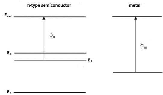
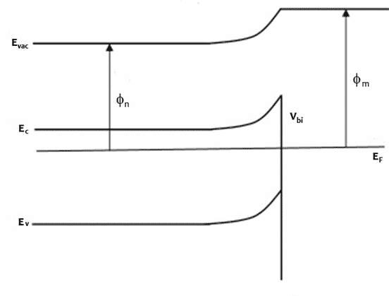
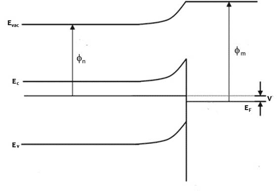
Figure 1 Energy band profiles of semiconductor/metal heterojunction, top before junction forms, middle, after junction forms and come to thermodynamic equilibrium, bottom under illumination, excited electrons accumulate in the n-type semiconductor, raising the electron Fermi level and generating a photovoltage, V
When illuminated with photons of energy greater than the band gap, electrons accumulate in the semiconductor side and holes in the metal side of the depletion region. The light splits the Fermi level and creates a photovoltage V equal to the difference in the Fermi levels of semiconductor and metal far from the junction.
The most common Schottky junction with graphene involves transferring a film of graphene onto an n-type silicon semiconductor [10, 11]. Due to the difference between the work functions of graphene and the semiconductor, a built-in potential forms in the semiconductor near the interface. When illuminated with energetic photons above the band gap, the photo-generated holes and electrons are separated and driven towards the graphene film and the semiconductor layer respectively by the built-in electric field (see Figure 2).
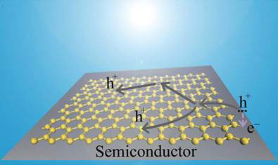
Figure 2 When illuminated, holes and electrons are generated in the semiconductor, with holes migrating to the graphene layer and holes towards semiconductor layer by the built-in electric field
Graphene-silicon ‘heterojunction’ solar cells in which single to few-layer graphene is transferred to a wafer of silicon, followed by chemical doping of the graphene, have reached efficiencies of 8.6 % or more [11].
Researchers at Peking University, National Center for Nanoscience and Technology, and Tsinghua University, all in Beijing, China, have recently shown that the efficiency of a graphene-silicon solar cell can be enhanced to 14.5 %, simply by spin-coating a thin layer of titanium oxide TiO2 on top of the graphene. The resulting TiO2-coated cell had much improved parameters (see Box 2): open-circuit voltage Voc 0.612 V, short-circuit current Jsc 32.5 mA/cm2, fill factor ff 72% and external quantum efficiency EQE up to 90 % across the visible region (Figure 3).
Box 2
Efficiency parameters of a solar cell
The performance of solar cells is characterized by a number of parameters.
Also important is the quantum efficiency:
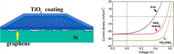
Figure 3 Titanium coating greatly improves performance of graphene-Si solar cell; left, schematic representation of the solar cell; right, variation of current J with voltage V
The monolayer graphene used was synthesized on copper foil substrate by the chemical vapour deposition (see [3]) and transferred to a n-type single-crystalline Si wafer covered with a 400 nm thick oxide. The graphene was doped with HNO3; then a colloid solution containing TiO2 nanoparticles 3-5 nm in diameter was spin-coated over the graphene and allowed to dry. This left tiny cracks in the TiO2 layer that exposed the graphene layer which was doped with more HNO3 acid. The uncoated cell was transparent, reflecting nearly 40% across the 400-1 100 nm range. After coating, it reflected only about 10 % of incident light in the visible spectrum (500-800 nm wavelength).
The original graphene-silicon cell had a Voc <0.4 V. After doping with HNO3 vapour, it increased to 0. 52 V and a higher ff of 65%, with current density Jsc essentially unchanged (see Figure 1 right). The power conversion efficiency PCE (see Box 2) reached 8.9 % after doping. But after coating with TiO2, Jsc was enhanced significantly from 23.9 to 32.5 mA/cm2. And Voc and ff were further improved by additional HNO3 doping.
Apart from reducing the amount of incident light reflected from the cell, the TiO2 coating also does not block acid treatment because it left cracks, and could allow introducing p-type (holes) doping of graphene, thereby enhancing Voc.
The TiO2-G-Si cell showed consistent performance under varying illumination intensity.
Article first published 24/07/13
Article first published 24/07/13
Comments are now closed for this article
There are 1 comments on this article.
Todd Millions Comment left 26th July 2013 20:08:43
Lepcon-A.Marks 1983.'sub micron rectenna'.If absorbing and rectifing structures can be doped to these structures-the results would be interesting too me.As well reports are-graphene is both super conducting,highly transperent,and 5 fold diamonds heat tranfer-all surely exellent features in a conducting top layer,that lets the light through,normally done by tin oxides-in normal solar cells.At the least the weight per watt should be dramatically dropable with these features.Thanx for this cheers.